Education
Beauty and Impactful Research Born in Nanotechnology Laboratory
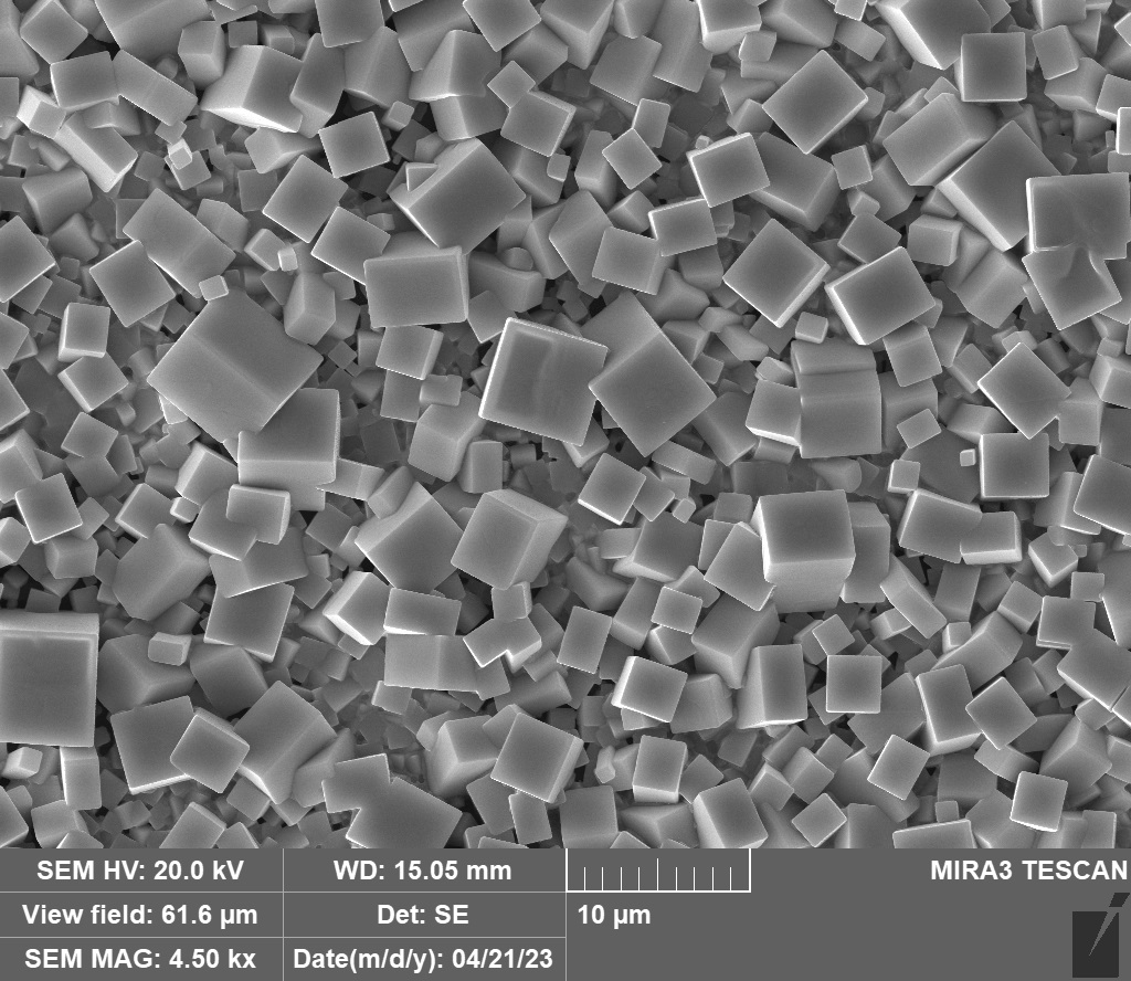
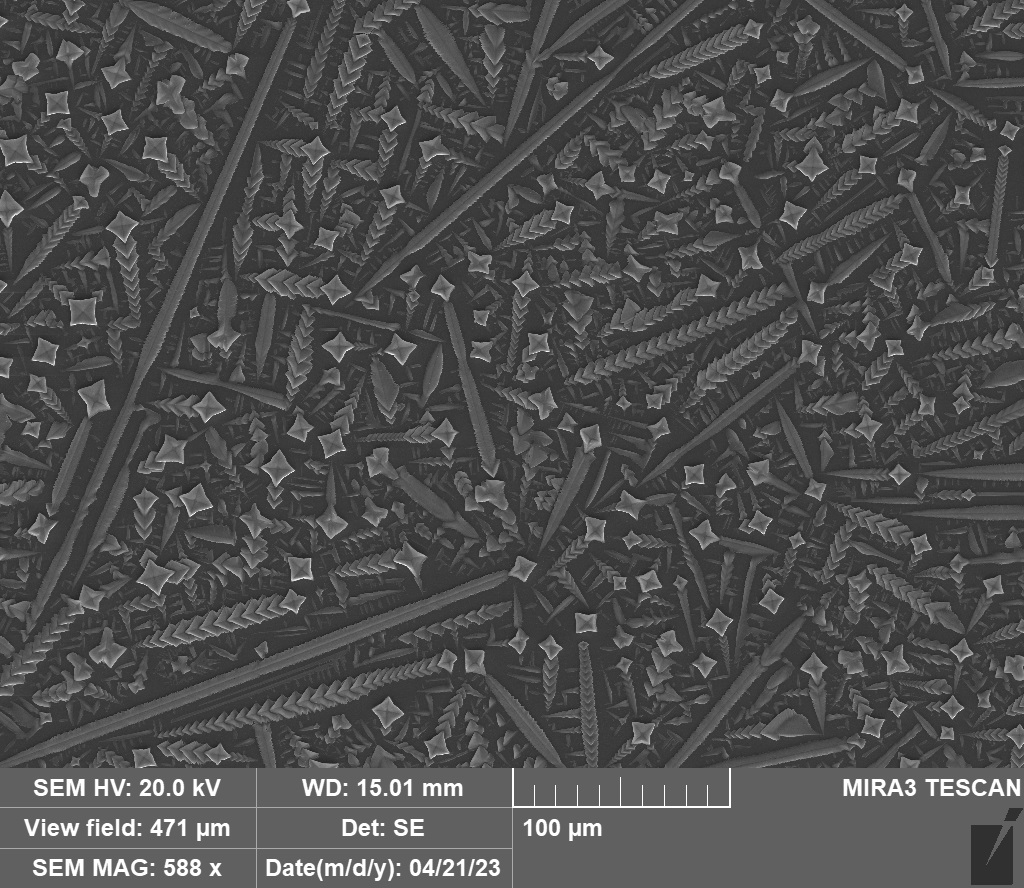
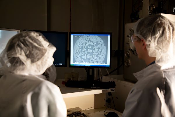
To the untrained eye, the breathtaking images generated in the Montana Tech Nanotechnology Laboratory (MTNL) resemble painted masterpieces possibly inspired by Pablo Picasso’s works in cubism—but to the students who created them, these micrographs hold much more critical data than that of simple abstract beauty. Clues about structure and composition can be gleaned to learn more about the optical, electronic, or mechanical properties of materials students work with, which could be critical building blocks to solving some of the world’s most pressing issues.
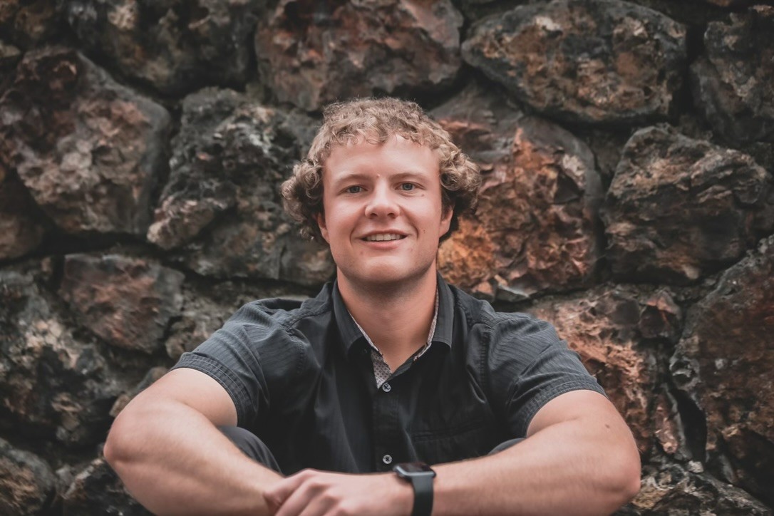
If you ask Materials Science Ph.D. student Xavier T. Vorhies if he’s doing science or making art in the lab, his answer is simple and direct.
“What we make, and do, is arguably an artform,” Vorhies said.
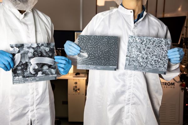
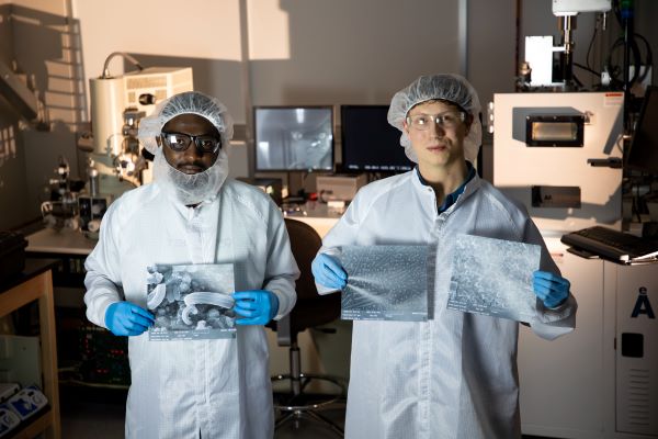
Vorhies, from Olney, Montana, and Earth Science and Engineering Ph.D. candidate Amos Taiswa, from Kilgoris, Kenya, recently won awards for their exceptional micrographs, or digital images taken through a microscope, presented at the International Conference on Electron, Ion and Photon Beam Technology and Nanofabrication (EIPBN). The EIPBN is the preeminent meeting for nanotechnology researchers and scientists from around the world, who come from academia, government, and industry to discuss recent trends and the future of small-scale phenomena and devices.
Each year, the EIPBN community holds a competitive micrograph contest. Investigations at the micro to nanoscale depend on microscopes to observe small-scale phenomena and morphologies and to evaluate performance. To highlight this important characterization method, the EIPBN micrograph contest seeks submissions that exhibit intrinsic beauty and/or excite curiosity. All entries were evaluated based on technical and artistic merit by a distinguished panel of judges.
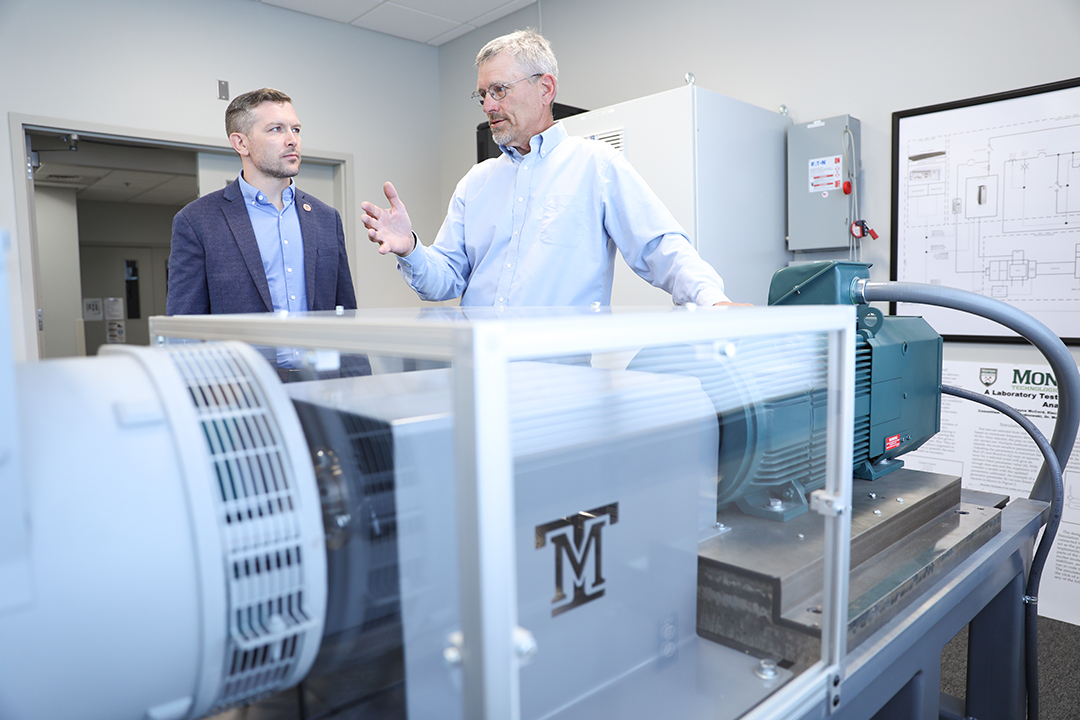
“The judging is done by some of the best nanotechnology scientists in the world,” said Dr. Jack Skinner, director of the MTNL, and head of the Department of Mechanical Engineering.
Vorhies won for the Best Electron Micrograph for his micrograph entitled The Wheat from the Chaff and the Grand Prize for his micrograph entitled Nano Cubism.
Taiswa won an honorable mention award for his micrograph entitled Banana Slug.
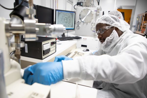
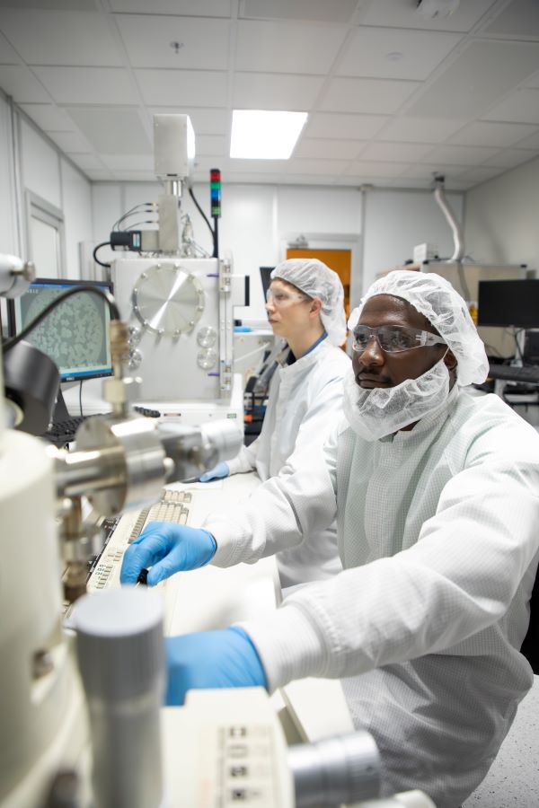
The images are the best each student has generated after countless hours in the laboratory’s clean room, which consists of a powerful scanning electron microscope and a transmission electron microscope protected by a locked door and air technology that limits particulate matter. Researchers who use the lab have to wear "bunny suits," white suits that cover them from head to toe and limit contamination.
“When working at the nano scale, one billionth of a meter, something as small as particles of dust or a stray piece of hair, could completely ruin your sample,” Vorhies said.
The processes Vorhies and Taiswa use to create their samples are fascinating. Vorhies grows materials used in solar cells called perovskites in a liquid solution on fragile thin sheets that are then inserted under the microscope. Taiswa uses a bioinspired method called electrospinning to create samples that mimic those of spiderwebs. His goal is to create materials that can be used for water purification.
“Where I grew up, there was scarcity, of everything, really,” Taiswa said. “I wanted to work on something that might provide a broader impact on building more sustainable communities.”
Taiswa notes that while the photos he and Vorhies submitted are artistically captivating, they don’t necessarily come from materials that were on target scientifically.
“Some are from failed experiments, but the micrographs look very interesting,” Taiswa said.
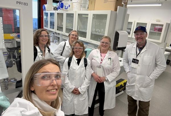
But every failure provides valuable information for future attempts. Both Taiswa and Vorhies have spent significant time in the nanotech lab, preparing and looking at their samples. They say easy access to high-powered electron microscopes helped attract them to Montana Tech. Students who work in the MTNL learn valuable skills that are highly competitive with much larger and more renowned institutions. In addition to electron microscopes in the MTNL, Tech is home to the Center for Advanced Materials Processing (CAMP), which has multiple scanning electron microscopes, and the Electron Microscopy Laboratory, which is home to a state-of-the-art Hitachi HT7820 scanning/transmission electron microscope that arrived on campus in May 2023, and is one of the most advanced instruments in the region. The Hitachi HT7820 was funded by a $1 million award from the National Science Foundation.
Vorhies said he was exposed to the electron microscope as an undergrad, which helped set him on the path to his Ph.D.
“We get a lot of recognition for our work at conferences, but that’s because of the amount of access and hands-on experience that we have in the laboratory,” Vorhies said.
Skinner said granting that kind of access to students has been a key part of a five-year effort to create and elevate the MTNL’s capabilities and recognition.
The laboratory has racked up a string of accolades and publications in its five years of existence.
In 2021, Materials Science Ph.D. student Luke Suttey won the EIPBN’s Grand Prize for his micrograph entitled Pretzel Sticks. The micrograph depicts electrospun polymer filters that were fabricated during the pandemic to accommodate the increased demand for novel mask materials. That same year Dr. Jessica Andriolo won the Most Bizarre micrograph for her image entitled Dr. Seuss Coloring Book, and an honorable mention for a second micrograph entitled Where’s Mickey?
Researchers have published work in The Journal of Vacuum Science and Technology B; The Journal of Physical Chemistry B; Water Supply, Coatings, Separation and Purification Technology; and MRS Communications, printed by the Cambridge University Press.
“I never would have thought we would be able to do this,” Skinner said. “We interact with peers all over the world. Our students go to conferences with these massive, internationally known schools and laboratories, they get job offers, they collaborate. That’s the goal. The goal is for us to be invited to the table and be a peer institution that brings something to the table.”
Skinner is a Butte native (B.S. General Engineering–Mechanical Option, ’00) who went on to get his M.S. degree from Washington State University, Pullman, WA, in Mechanical Engineering in 2002, and a Ph.D. from the University of California, Davis, CA, in Mechanical Engineering in 2007. He was a graduate student researcher at the Berkeley Sensor and Actuator Center (BSAC) at the University of California, Berkeley from 2004 to 2007, where he developed diffractive optical microsystems. From 2003 to 2012, he was with Sandia National Laboratories in Livermore, California.
While Skinner had to leave Butte to find more opportunities, he hopes students like Vorhies and Taiswa see the Mining City as a potential long-term home for their scientific endeavors, rather than leaving for Silicon Valley or another major international city.
“If you don’t want to leave Butte, you don’t have to leave,” Skinner said. “We’re working on proposals that would help build the local economy. We patent our work. We are here to change things, and offer more to our students, to our community.”
Vorhies would like to work for a national laboratory as a scientific researcher, and Taiswa has a plan to perhaps stick around Butte a little longer before tackling a lifelong dream: of pursuing a political career in his home country of Kenya.
“Our students can go anywhere and be successful,” Skinner said.